
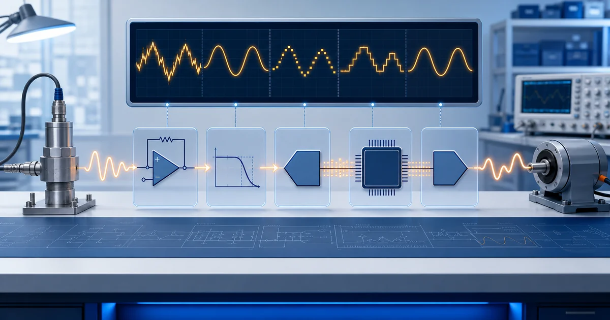
Select an analog signal chain by translating the signal, accuracy, speed, environment and procurement requirements into limits for every stage. A converter’s bit count is only a starting point. Analog Devices shows that a 12-bit ADC with 4 LSB of integral nonlinearity can provide only about 10-bit accuracy, even after offset and gain calibration (Analog Devices, The ABCs of Analog to Digital Converters, 2002).
This guide turns those requirements into reviewable filters for ADCs, DACs, amplifiers, drivers, references, interfaces, packages and lifecycle status. It serves design engineers and purchasing teams working from one controlled worksheet. It is a documentation-based review of official manufacturer material, not a claim of laboratory characterization, compatibility testing or product availability.
How should system requirements define an analog signal chain?
Start with the signal and required system result, then assign limits to each stage. Analog Devices’ 2002 ADC guidance begins with conversion rate, supply, input range and channel count before analyzing accuracy (The ABCs of Analog to Digital Converters, 2002). That order prevents a strong converter from entering the wrong architecture.
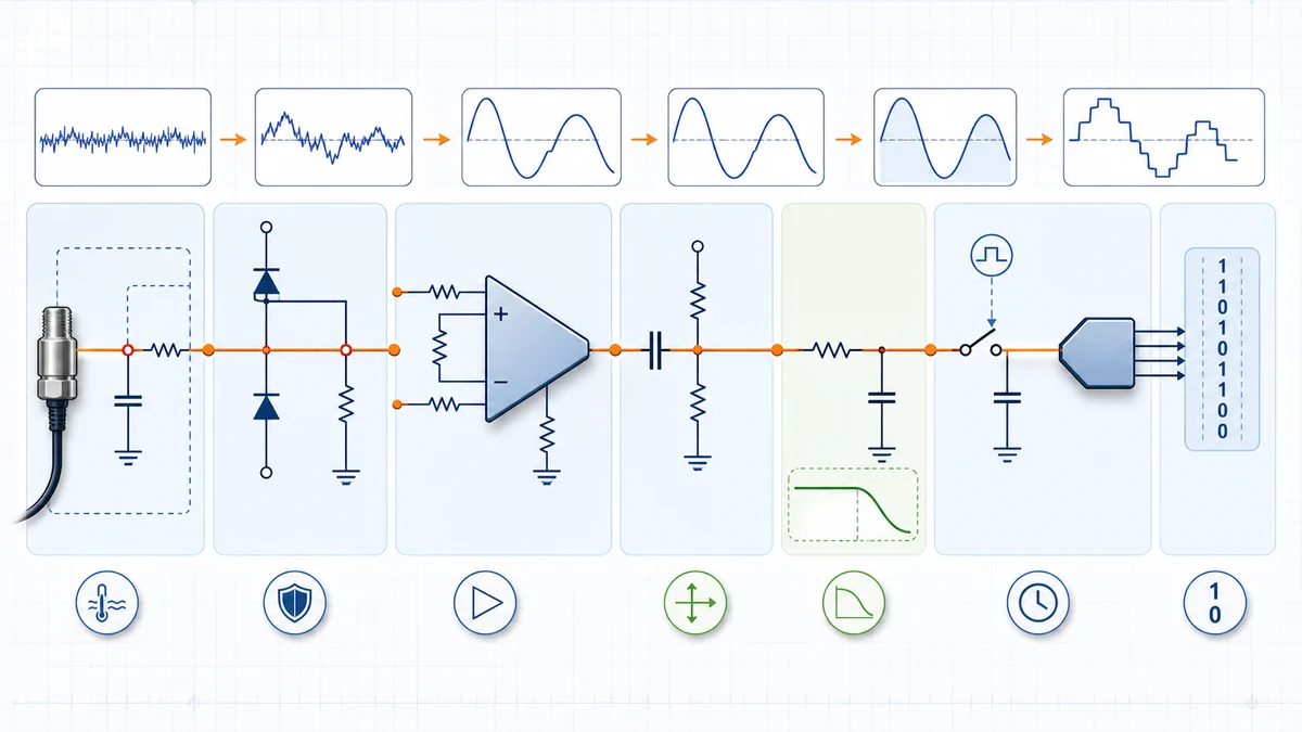
Capture the signal envelope
Record minimum and maximum input, common-mode range, source impedance, polarity and overload behavior. Add signal bandwidth, highest input frequency, channel count and multiplexing sequence. A small sensor signal may need instrumentation gain before filtering. A larger bipolar signal may instead need attenuation, level shifting or protection before it reaches the converter input.
Define the result, not only the nominal bits
Write the required total unadjusted error, noise, dynamic range, latency and update rate at the system output. State the operating temperature range and calibration plan. If firmware can remove offset and gain, preserve the residual errors and lost input range in the worksheet. INL, drift, reference noise and settling generally remain separate concerns.
How do you build a defensible analog error budget?
Use worst-case addition for a guaranteed boundary; reserve root-sum-square for terms that are demonstrably uncorrelated. Analog Devices makes that distinction explicit in its ADC error guidance (The ABCs of Analog to Digital Converters, 2002). Qualification records can retain both totals.
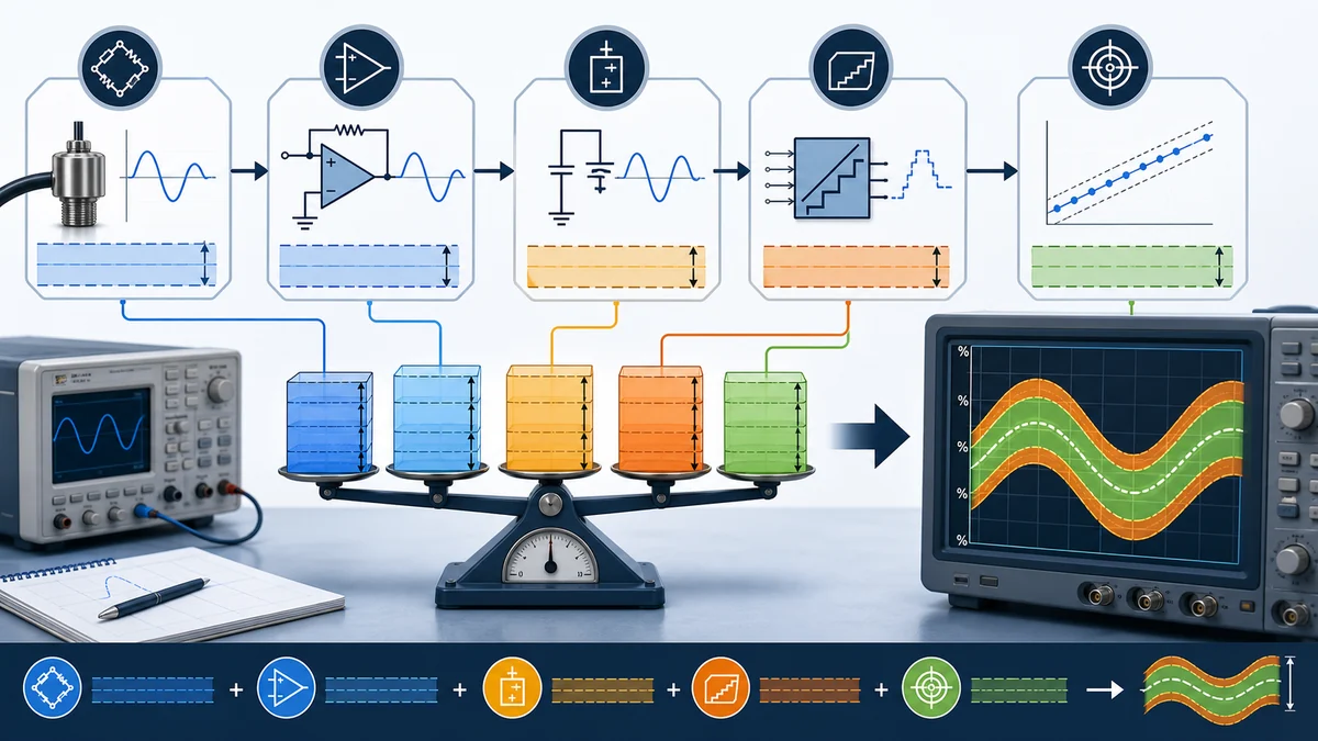
Refer all contributions to one domain: input volts, output volts, full-scale percentage or ppm. Preserve the specified test condition and label each value as maximum, typical or derived. A mixed column of typical noise and guaranteed INL cannot support a defensible limit.
Separate correctable and residual terms
Two-point calibration can remove offset and gain under controlled conditions, but it cannot recover clipping. Nonlinearity, drift, aging, bias effects and reference loading require separate allowances. Add production spread, instrumentation uncertainty and uncovered environmental corners.
Place a datasheet table, revision and condition beside every budget row. That evidence trail exposes weak assumptions before qualification and makes later PCN, alternate-source or supplier reviews reproducible.
Which ADC architecture and specifications fit the measurement?
Fix bandwidth, latency, channel behavior and usable accuracy before choosing an ADC architecture. TI describes ADC0804-N as an 8-bit, single-channel parallel SAR device rated to 10 ksps (ADC0804-N product page, accessed 2026). That profile is one bounded example, not a modern default.
| System need | First conversion path to examine | Verification focus |
|---|---|---|
| Low-bandwidth precision sensor | Sigma-delta ADC or precision SAR ADC | Latency, noise, drift, rejection and input drive |
| Multiplexed channels with bounded latency | SAR ADC | Acquisition time, channel settling and throughput |
| Wideband sampled signal | Pipeline or high-speed ADC | SNR, SFDR, clock jitter and input frequency |
| Accurate static control voltage | Voltage-output precision DAC | INL, offset, gain, reference and load stability |
| Programmable current or multiplying function | Current-output or multiplying DAC | Reference drive, compliance and external I/V stage |
Next verify input topology, common-mode window, full-scale span, reference scheme and missing-code guarantee. DC work needs DNL, INL, offset, gain and drift; sampled waveforms add SNR, SINAD, SFDR and aperture-jitter constraints. Multiplexing introduces large channel steps, whereas simultaneous conversion adds matching and skew.
The catalog entries for ADC0804LCN and ADC0809CCN help locate historical documentation. They do not prove interchangeability, stock or current orderable status.
How should the amplifier, ADC driver and RC filter be selected?
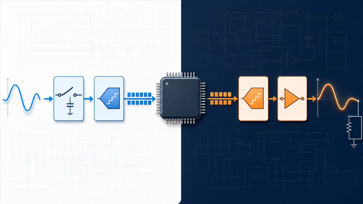
Derive the front end from acquisition time, input step and permitted settling residue. In Analog Devices’ AD7960 example, a 100 ns acquisition interval yields first-order targets of 40 MHz bandwidth, 100 V/µs slew rate, 100 ns settling and 105.5 dB driver SNR (Selecting an ADC Driver, 2015). These are worked-example results, not universal minima.
Treat the sampling input as a switched load
SAR charge kickback interacts with output impedance, the isolation resistor and filter capacitance. Analog Devices’ 2012 front-end note requires the RC network to suppress broadband noise without consuming the available settling interval (Front-End Amplifier and RC Filter Design). Evaluate the largest multiplexer step, capacitive stability, layout parasitics and source resistance.
Match topology to the transducer
Instrumentation gain, level translation and active filtering impose different swing, bias-current, rejection and distortion limits. ICEARTH pages for INA118P, AD620AN and TL074CN identify catalog devices; none endorses a particular sensor or converter. Simulate the selected network, then verify production-intent hardware across process, supply and temperature.
How should the voltage reference and its buffer be chosen?
Select the reference as a dynamic circuit element, not a quiet nominal voltage. In an Analog Devices AD7980 example at 1 MSPS and 5 V, reference current shows spikes near 2.5 mA versus about 330 µA typical average current (Voltage Reference Design for Precision Successive-Approximation ADCs, 2013). Local energy storage and buffer stability therefore matter.
Screen initial accuracy, temperature coefficient, aging, low-frequency noise, wideband noise, load regulation, source-sink capability and shared-load coupling. Ratiometric sensing cancels only documented common errors.
Analog Devices recommends a low-ESR reservoir capacitor, typically 10 µF or more, close to the AD7980 reference input in its example (Voltage Reference Design for Precision Successive-Approximation ADCs, 2013). Larger capacitance can reduce transient burden, but it may destabilize a buffer. Use the specified capacitor range, ESR and compensation network for the selected parts.
How do DAC architecture and the output stage affect selection?
Select a DAC by required output type, settling, load, monotonicity and total chain error. Texas Instruments lists the active DAC0800 family as an 8-bit current-output multiplying DAC with 100 ns typical settling (Texas Instruments, DAC0800 product page, retrieved 2026). Its external reference and current output require an I/V stage and reference-loading review.
A voltage-output DAC may simplify a lightly loaded control node, yet output swing and stability can change with capacitive or resistive loads. A current-output DAC provides different compliance and conversion options but needs a transimpedance stage or suitable load. Check code-dependent glitch, settling definition, zero-scale behavior and power-up state against the application sequence.
The DAC error budget includes more than INL. Analog Devices identifies DAC, reference and op-amp contributions and recommends RSS for normally uncorrelated terms (How to Best Calculate the Digital-to-Analog Converter Signal Chain Error Budget, 2021). When a guaranteed boundary matters, retain a worst-case total beside the RSS estimate.
The DAC0800LCN catalog page identifies a historical ordering string for document review. Do not shorten it in a BOM or infer identity with a current TI orderable code. Package, finish, lifecycle and manufacturer remain controlled attributes.
Discrete and integrated signal chain tradeoffs
Choose discrete stages for topology control. Choose integration when density and pre-optimized interactions outweigh customization. A 2026 Analog Devices article compares a signal chain µModule with 15 to 40-plus discrete parts and reports about an 11-fold footprint reduction for its example (Analog Devices EngineerZone article, 2026).
Discrete stages preserve topology freedom, unusual ranges and multi-source planning, but leave matching, kickback, grounding, thermal gradients and reference recovery on the PCB. Integration can reduce those interactions; fixed gains, input limits, package choices and single-source exposure still need the same error-budget review.
How should interface, package, lifecycle and order codes be screened?
Release the complete manufacturer orderable code, never a family shorthand. TI marks exact INA118P, an 8-pin PDIP, as Last Time Buy (INA118P part details, accessed 2026). Analog Devices lists the 8-lead PDIP AD620ANZ as Production (AD620 product page, accessed 2026).
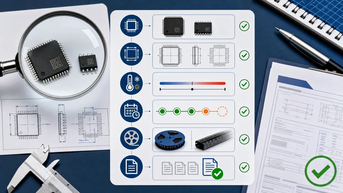
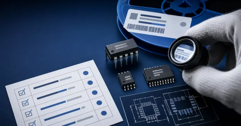
Digital acceptance covers logic thresholds, framing, clock polarity, setup, hold, data-ready behavior, reset defaults and isolation direction. Physical review compares the controlled drawing, land pattern, pitch, height, exposed pad, moisture level, finish, grade and carrier orientation.
Pin-number functions for INA118P and INA818 align, but current INA818 orderables use SOIC while exact INA118P uses PDIP. That footprint change, plus electrical differences, requires redesign and qualification. Likewise, legacy AD620AN must not be merged with AD620ANZ, and ADC0804LCN must not be silently normalized to a current /NOPB identity.
Analog signal chain release worksheet
| Worksheet field | Requirement to record | Evidence needed before release |
|---|---|---|
| Signal source | Range, common mode, impedance, faults | Sensor and protection specifications |
| Accuracy | Total error, noise, drift, calibration | Error budget with units and conditions |
| Timing | Bandwidth, sample rate, latency, settling | Converter and driver timing limits |
| ADC | Architecture, channels, input, interface | Current datasheet and ordering table |
| Driver and filter | Gain, noise, slew, stability, RC values | Simulation plus planned bench tests |
| Reference | Accuracy, drift, noise, transient load | Reference and buffer stability data |
| DAC and output | Output type, load, settling, startup | Full-chain error and load analysis |
| Digital interface | Levels, timing, framing, isolation | Host and converter timing review |
| Physical identity | Package, pinout, grade, finish, packing | Drawing and exact manufacturer code |
| Lifecycle | Status, PCN/PDN, approved alternate plan | Dated manufacturer lifecycle evidence |
| Validation | Corner cases and acceptance limits | Test plan, equipment and traceability |
Engineering and purchasing should sign the same worksheet revision. Proposed alternates return to affected performance, package and lifecycle rows instead of entering the BOM through a family-name match.
Frequently asked questions
These questions cover the specification, driver, reference, interface and exact-order-code checks that commonly change a signal-chain decision.
Does a 12-bit ADC provide 12-bit accuracy?
No. Resolution counts codes; accuracy also includes INL, offset, gain, reference, drift, noise and settling. Analog Devices shows 4 LSB INL limiting one 12-bit example to roughly 10-bit accuracy.
How much bandwidth does an ADC driver need?
No fixed multiplier works. Calculate bandwidth, slew and settling from the acquisition interval, voltage step and residual-error target. The cited AD7960 example produces a 40 MHz estimate for 100 ns, but its equations remain first-order approximations.
Can INA818 replace INA118P without a board change?
No drop-in claim is justified. Functional pin numbers align, yet exact INA118P is PDIP and current INA818 devices are SOIC. Recheck footprint, supply range, gain equation, common-mode behavior, protection, output swing and qualification limits.
Should an error budget use RSS or worst-case addition?
Worst-case addition supplies a guaranteed bound. RSS is appropriate only for reasonably uncorrelated contributions. Retaining both totals separates qualification margin from the expected combination of independent random effects.
Is a family name sufficient on an RFQ?
No. Specify manufacturer, exact part number, quantity, package, grade, packing and destination. Preserve suffixes on the quotation and incoming label; AD620AN versus AD620ANZ illustrates why automatic normalization is unsafe.
Qualification should exercise brownout recovery, overvoltage clamping, reverse-polarity protection, dielectric absorption, crosstalk, alias rejection, ground bounce, clock feedthrough, latch-up immunity, warm-up drift, startup determinism, shielding continuity, connector leakage, EMI susceptibility, ESD survival and firmware timeout behavior.
Sources, verification method and review cadence
This documentation review uses 13 official manufacturer resources. Each link was accessed 29 July 2026. Recheck revisions, package drawings and PCN or PDN notices before release; no statement here represents laboratory characterization, authenticity inspection, inventory or compatibility testing.
- ADI: ADC errors and system performance (2002-07-22).
- ADI: optimized ADC driver selection (2015-07-13).
- ADI: precision SAR front-end RC design (2012-12).
- ADI: voltage references for SAR converters (2013-06).
- ADI: DAC chain error budgeting (2021-03-23).
- TI: DAC0800 product record.
- TI: DAC0800/DAC0802 datasheet.
- TI: ADC0804-N product record.
- TI: ADC0804-N Rev. C datasheet.
- TI: INA118P orderable details.
- TI: INA118 Rev. C datasheet.
- ADI: AD620 product models and datasheet.
- ADI EngineerZone: discrete versus signal-chain µModule (2026-07-07).
Archive the worksheet, assumptions, document revisions and corner-test plan with the BOM. Revalidate production hardware under intended source, load, supply, temperature and firmware conditions.
Request an analog component quote
Continue the engineering review
From this guide to exact component data
Related component comparisons
These comparisons contain an exact product record linked in this article.
Browse product recordsAll engineering guidesSourcing resources