
JS28F128P33BF70A
128 Mbit parallel NOR flash memory with x8/x16 interface
Key details
| Part Number | JS28F128P33BF70A |
|---|---|
| Manufacturer | Micron Technology (Intel/Numonyx legacy) |
| Category | Parallel NOR Flash |
| Lifecycle Status | Obsolete |
| Series | P33 |
| Package / Case | 56-pin TSOP-I |
| Pin Count | 56 |
| Operating Temperature | -40°C to +85°C; confirm suffix grade |
| Last Verified | 2026-07-22 |
Part information
JS28F128P33BF70A Overview
JS28F128P33BF70A is a Micron Technology (Intel/Numonyx legacy) 128 Mbit parallel NOR flash memory with x8/x16 interface supplied in 56-pin TSOP-I. This page uses the exact orderable code because package, grade, temperature and option suffixes can change compatibility.
Key Technical Specifications
| Density | 128 Mbit |
|---|---|
| Interface | Asynchronous parallel x8/x16 |
| Architecture | Bottom-boot block architecture |
| Access Time | 70 ns |
| Supply Class | 1.8 V core / 3 V I/O class |
Package and Ordering Notes
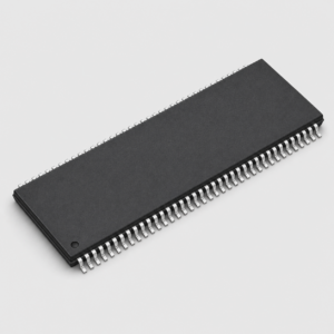
The listed package is 56-pin TSOP-I with 56 pins, leads, lands or contacts. The featured image is a generic package illustration for form-factor identification and is not an actual date-code or lot photograph. Lifecycle is recorded as Obsolete; confirm current factory support and last-time-buy constraints before design-in.
Sourcing Guidance
JS28F128P33BF70A is obsolete or discontinued. Require traceability, date-code, package-marking and storage-condition checks for remaining stock.
For an accurate quotation, include the full MPN, target quantity, acceptable date-code range, packaging format and destination. Icearth can help review traceability documents, label photos and electrical/package alignment before order placement.
Manufacturer Documentation
Technical values were checked against Micron Technology (Intel/Numonyx legacy) documentation. Use the linked datasheet as the controlling source and re-check revisions before PCB release or firmware qualification.
JS28F128P33BF70A FAQ
What is JS28F128P33BF70A?
JS28F128P33BF70A is a Micron Technology (Intel/Numonyx legacy) 128 Mbit parallel NOR flash memory with x8/x16 interface. It belongs to the P33 series.
What are the key specifications of JS28F128P33BF70A?
Density is 128 Mbit, and Interface is Asynchronous parallel x8/x16. Use the linked manufacturer datasheet for limits, test conditions and revision-controlled values.
What package does JS28F128P33BF70A use?
JS28F128P33BF70A is supplied in 56-pin TSOP-I with 56 pins, leads, lands or contacts. Verify the exact footprint and ordering suffix before PCB release.
Is JS28F128P33BF70A still in production?
JS28F128P33BF70A is obsolete or discontinued. Any remaining stock should be checked for traceability, date code, package marking and storage history.
What should be checked before sourcing JS28F128P33BF70A?
Confirm the complete MPN, electrical ratings, package, temperature grade and required quantity. Possible alternatives include Select a current parallel NOR flash after verifying command set, boot-block layout, voltage, timing and TSOP pinout, but compatibility must be verified independently.
How JS28F128P33BF70A differs from related orderable parts
JS28F128P33BF70A belongs to the P33 family. Compared with JS28F128P33TF70A, the recorded differences include Architecture: Bottom-boot block architecture rather than Top-boot block architecture. A shared family name does not establish pin, firmware or qualification compatibility.
| Part number | Recorded function | Package | Pins / contacts | Temperature | Lifecycle |
|---|---|---|---|---|---|
| JS28F128P33BF70A | 128 Mbit parallel NOR flash memory with x8/x16 interface | 56-pin TSOP-I | 56 pins, leads or contacts | -40°C to +85°C; confirm suffix grade | Obsolete |
| JS28F128P33TF70A | 128 Mbit parallel NOR flash memory with x8/x16 interface | 56-pin TSOP-I | 56 pins, leads or contacts | -40°C to +85°C; confirm suffix grade | Obsolete |
| JS28F256P33BFE | 256 Mbit parallel NOR flash memory with x8/x16 interface | 56-pin TSOP-I | 56 pins, leads or contacts | -40°C to +85°C; confirm suffix grade | Obsolete |
| JS28F256P33TFE | 256 Mbit parallel NOR flash memory with x8/x16 interface | 56-pin TSOP-I | 56 pins, leads or contacts | -40°C to +85°C; confirm suffix grade | Obsolete |
For an RFQ or AVL review, quote the complete JS28F128P33BF70A code and verify the manufacturer ordering table, package drawing, packing method and revision. The related numbers above are comparison references, not declared drop-in replacements.
Exact order-code identity for JS28F128P33BF70A
For BOM, label, AVL and RFQ matching, preserve these visible code segments: opening alphabetic sequence JS; middle numeric sequence two eight; middle alphabetic sequence F; middle numeric sequence one two eight; middle alphabetic sequence P; middle numeric sequence three three; middle alphabetic sequence BF; middle numeric sequence seven zero; and terminal alphabetic sequence A. The nearest published comparison codes are JS28F128P33TF70A; JS28F256P33BFE; and JS28F256P33TFE. Compare every segment because a changed character can identify a different density, voltage, package, temperature, qualification or packing option.
Do not shorten the requested code to P33 or remove its terminal characters. Ask the supplier to reproduce the complete code on the quotation and provide label or traceability evidence when exact suffix matching is mandatory.
JS28F128P33BF70A specification interpretation
The following notes interpret the recorded values for this exact orderable code. They are intended to make model-to-model differences visible during engineering and procurement review; the manufacturer datasheet remains the controlling source.
- Density: The recorded value is 128 Mbit, expressed in words as one hundred twenty eight Mbit. Confirm address organization, software support and required usable capacity.
- Interface: The recorded value is Asynchronous parallel x8/x16, expressed in words as Asynchronous parallel xeight/xsixteen. Confirm logic levels, signaling mode, host support and required external components.
- Architecture: The recorded value is Bottom-boot block architecture. Confirm the value and its datasheet test conditions for the exact ordering suffix. The comparison record for JS28F128P33TF70A lists Top-boot block architecture; this page therefore preserves Bottom-boot block architecture as the value associated with JS28F128P33BF70A.
- Access Time: The recorded value is 70 ns, expressed in words as seventy ns. Confirm system timing margin and the test conditions attached to the published limit.
- Supply Class: The recorded value is 1.8 V core / 3 V I/O class, expressed in words as one point eight V core / three V I/O class. Check rail compatibility, tolerance and sequencing under worst-case conditions.
Choosing between JS28F128P33BF70A and JS28F128P33TF70A
The decision points below use the values recorded for these two exact orderable codes. Select JS28F128P33BF70A when its stated value is the BOM requirement; select JS28F128P33TF70A only when the alternate value has been independently approved.
- Architecture: JS28F128P33BF70A records Bottom-boot block architecture, while JS28F128P33TF70A records Top-boot block architecture. Confirm the value and its datasheet test conditions for the exact ordering suffix.
If the assembly documentation names JS28F128P33BF70A, require the quotation and supplied label to retain JS28F128P33BF70A in full. A request for JS28F128P33TF70A should be handled as a proposed substitution and reviewed for electrical, mechanical, firmware and qualification impact before approval.
Lifecycle and sourcing review
This part has a legacy lifecycle status. Submit the exact MPN, quantity, delivery destination and date-code requirements for a sourcing review.
JS28F128P33BF70A is obsolete or discontinued. Require traceability, date-code, package-marking and storage-condition checks for remaining stock.
Potential alternative part numbers
Verify package, pinout, voltage, firmware behavior and qualification before substitution.