
MX25L51245GXDI-10G
512Mb 3V high-performance SPI multi-I/O NOR Flash
Key details
| Part Number | MX25L51245GXDI-10G |
|---|---|
| Manufacturer | Macronix |
| Category | Serial NOR Flash |
| Lifecycle Status | Production |
| Series | MX25L51245G |
| Package / Case | 24-BGA (5x5 ball array) |
| Pin Count | 24 |
| Operating Temperature | -40°C to +85°C (Industrial) |
| Last Verified | 2026-07-17 |
Part information
MX25L51245GXDI-10G Overview
MX25L51245GXDI-10G is a Macronix 512Mb 3V high-performance SPI multi-I/O NOR Flash supplied in 24-BGA (5×5 ball array). This page uses the exact orderable code because package, speed, temperature and option suffixes can change compatibility.
Key Technical Specifications
| Memory Density | 512Mb |
|---|---|
| Interface | SPI / Dual / Quad I/O / QPI |
| Supply Voltage | 2.7V to 3.6V |
| Features | DTR, SFDP, suspend/resume, advanced protection |
| Addressing | 4-byte addressing supported |
| Package | 24-BGA, 5×5 ball array |
| Temperature Grade | Industrial, -40°C to +85°C |
Package and Ordering Notes
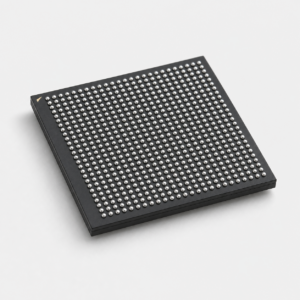
The listed package is 24-BGA (5×5 ball array) with 24 pins/lands/balls. The featured image is a generic package illustration for form-factor identification and is not an actual date-code or lot photograph. The family is listed by Macronix as Production at the verification date.
Sourcing Guidance
Confirm XD package code, 24-ball 5×5 array, -10G speed option and 3V interface. Review ball map and PCB land pattern rather than relying on density-family similarity.
For an accurate quotation, include the full MPN, target quantity, acceptable date-code range, packaging format and destination. Icearth can help review traceability documents, label photos and electrical/package alignment before order placement.
Manufacturer Documentation
Technical values were checked against Macronix documentation. Use the linked datasheet as the controlling source and re-check revisions before PCB release or firmware qualification.
MX25L51245GXDI-10G selection and design context
MX25L51245GXDI-10G is cataloged as a Serial NOR Flash in the MX25L51245G family. Its recorded function is 512Mb 3V high-performance SPI multi-I/O NOR Flash. Selection should be based on the complete electrical limits, package drawing and ordering suffix rather than the abbreviated family code.
- Memory Density: 512Mb. Confirm address organization, software support and required usable capacity.
- Interface: SPI / Dual / Quad I/O / QPI. Confirm logic levels, signaling mode, host support and required external components.
- Supply Voltage: 2.7V to 3.6V. Check rail compatibility, tolerance and sequencing under worst-case conditions.
- Features: DTR, SFDP, suspend/resume, advanced protection. Confirm the value and its datasheet test conditions for the exact ordering suffix.
Application and qualification considerations
When evaluating this memory device, confirm density, organization, interface mode, supply rails, access or clock timing, erase endurance and software command compatibility. For a new design, review power-up behavior, interface timing, absolute maximum ratings, thermal limits and any external-component requirements in the latest manufacturer documentation. Existing-board replacement work should additionally confirm pinout, footprint, firmware assumptions and qualification grade.
Procurement checks for MX25L51245GXDI-10G
The recorded package is 24-BGA (5×5 ball array), the temperature range is -40°C to +85°C (Industrial), and the lifecycle status is Production as of 2026-07-17. Before ordering, confirm the exact MPN on the label, packing format, quantity, date-code requirements, traceability documents and current factory status.
MX25L51245GXDI-10G FAQ
What distinguishes MX25L51245GXDI-10G within the MX25L51245G family?
MX25L51245GXDI-10G is the exact orderable code for a 512Mb 3V high-performance SPI multi-I/O NOR Flash in 24-BGA (5×5 ball array). Related MX25L51245G devices may change package, rating, interface option or qualification grade, so compare the manufacturer ordering table before substitution.
What package and footprint checks are required for MX25L51245GXDI-10G?
MX25L51245GXDI-10G is recorded in 24-BGA (5×5 ball array) with 24 pins, leads or contacts. Confirm the manufacturer package drawing, dimensions, pin numbering, exposed-pad requirements and packing suffix before releasing a PCB footprint.
Which specifications should be verified when selecting MX25L51245GXDI-10G?
Memory Density is recorded as 512Mb, Interface is recorded as SPI / Dual / Quad I/O / QPI. Use the latest datasheet for minimum and maximum limits, test conditions, timing and absolute maximum ratings rather than relying only on a distributor summary.
What is the lifecycle status of MX25L51245GXDI-10G?
MX25L51245GXDI-10G was recorded as Production when verified on 2026-07-17. Reconfirm factory status, revision availability, lead time and any last-time-buy notice before design-in or volume procurement.
What information should be included in an RFQ for MX25L51245GXDI-10G?
Provide the complete MX25L51245GXDI-10G orderable code, target quantity, acceptable date-code range, required packing method, delivery destination and documentation needs. For replacement work, also identify the existing package and any mandatory qualification grade.
Lifecycle and sourcing review
Lifecycle information is shown for reference. Confirm current manufacturer documentation, availability and technical suitability before purchase.
Confirm XD package code, 24-ball 5x5 array, -10G speed option and 3V interface. Review ball map and PCB land pattern rather than relying on density-family similarity.